- 您现在的位置:买卖IC网 > Sheet目录334 > ISL6610IRZ (Intersil)IC MOSFET DRVR DUAL SYNC 16-QFN
�� �
�
�ISL6610,� ISL6610A�
�Timing� Diagram�
�2.5V�
�PWM�
�t� PDHU�
�t� PDLU�
�t� TSSHD�
�UGATE�
�LGATE�
�1V�
�t� RU�
�1V�
�t� RL�
�t� PTS�
�t� TSSHD�
�t� RU�
�t� FU�
�t� PTS�
�t� PDLL�
�t� PDHL�
�t� FL�
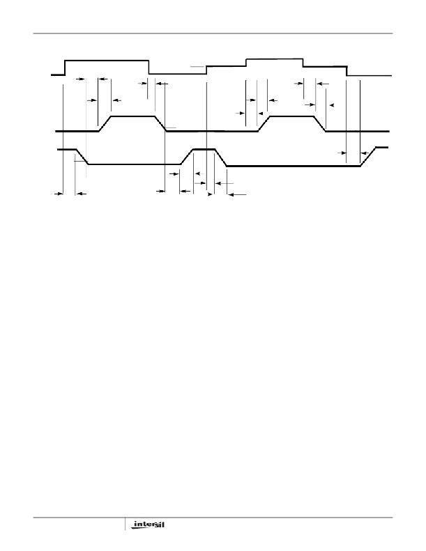
�FIGURE� 1.� TIMING� DIAGRAM�
�Operation� and� Adaptive� Shoot-Through� Protection�
�Designed� for� high� speed� switching,� the� ISL6610,� ISL6610A�
�MOSFET� driver� controls� both� high-side� and� low-side� N-�
�Channel� FETs� from� one� externally� provided� PWM� signal.�
�A� rising� transition� on� PWM� initiates� the� turn-off� of� the� lower�
�MOSFET� (see� Figure� 1).� After� a� short� propagation� delay�
�[t� PDLL� ],� the� lower� gate� begins� to� fall.� Typical� fall� times� [t� FL� ]�
�are� provided� in� the� Electrical� Specifications� .� Adaptive� shoot-�
�through� circuitry� monitors� the� LGATE� voltage� and� turns� on�
�the� upper� gate� following� a� short� delay� time� [t� PDHU� ]� after� the�
�LGATE� voltage� drops� below� ~1V.� The� upper� gate� drive� then�
�begins� to� rise� [t� RU� ]� and� the� upper� MOSFET� turns� on.�
�A� falling� transition� on� PWM� indicates� the� turn-off� of� the� upper�
�MOSFET� and� the� turn-on� of� the� lower� MOSFET.� A� short�
�propagation� delay� [t� PDLU� ]� is� encountered� before� the� upper�
�gate� begins� to� fall� [t� FU� ].� The� adaptive� shoot-through� circuitry�
�monitors� the� UGATE-PHASE� voltage� and� turns� on� the� lower�
�MOSFET� a� short� delay� time,� t� PDHL� ,� after� the� upper�
�MOSFET’s� gate� voltage� drops� below� 1V.� The� lower� gate� then�
�rises� [t� RL� ],� turning� on� the� lower� MOSFET.� These� methods�
�prevent� both� the� lower� and� upper� MOSFETs� from� conducting�
�simultaneously� (shoot-through),� while� adapting� the� dead�
�time� to� the� gate� charge� characteristics� of� the� MOSFETs�
�being� used.�
�This� driver� is� optimized� for� voltage� regulators� with� large� step�
�down� ratio.� The� lower� MOSFET� is� usually� sized� larger�
�compared� to� the� upper� MOSFET� because� the� lower�
�MOSFET� conducts� for� a� longer� time� during� a� switching�
�period.� The� lower� gate� driver� is� therefore� sized� much� larger�
�to� meet� this� application� requirement.� The� 0.4� Ω� on-resistance�
�and� 4A� sink� current� capability� enable� the� lower� gate� driver� to�
�6�
�absorb� the� current� injected� into� the� lower� gate� through� the�
�drain-to-gate� capacitor� (C� GD� )� of� the� lower� MOSFET� and�
�help� prevent� shoot� through� caused� by� the� self� turn-on� of� the�
�lower� MOSFET� due� to� high� dV/dt� of� the� switching� node.�
�Tri-State� PWM� Input�
�A� unique� feature� of� the� ISL6610,� ISL6610A� is� the� adaptable�
�tri-state� PWM� input.� Once� the� PWM� signal� enters� the�
�shutdown� window,� either� MOSFET� previously� conducting� is�
�turned� off.� If� the� PWM� signal� remains� within� the� shutdown�
�window� for� longer� than� 80ns� of� the� previously� conducting�
�MOSFET,� the� output� drivers� are� disabled� and� both� MOSFET�
�gates� are� pulled� and� held� low.� The� shutdown� state� is�
�removed� when� the� PWM� signal� moves� outside� the� shutdown�
�window.� The� PWM� rising� and� falling� thresholds� outlined� in�
�the� Electrical� Specifications� determine� when� the� lower� and�
�upper� gates� are� enabled.� During� normal� operation� in� a�
�typical� application,� the� PWM� rise� and� fall� times� through� the�
�shutdown� window� should� not� exceed� either� output’s� turn-off�
�propagation� delay� plus� the� MOSFET� gate� discharge� time� to�
�~1V.� Abnormally� long� PWM� signal� transition� times� through�
�the� shutdown� window� will� simply� introduce� additional� dead�
�time� between� turn� off� and� turn� on� of� the� synchronous�
�bridge’s� MOSFETs.� For� optimal� performance,� no� more� than�
�100pF� parasitic� capacitive� load� should� be� present� on� the�
�PWM� line� of� ISL6610,� ISL6610A� (assuming� an� Intersil� PWM�
�controller� is� used).�
�Bootstrap� Considerations�
�This� driver� features� an� internal� bootstrap� diode.� Simply�
�adding� an� external� capacitor� across� the� BOOT� and� PHASE�
�pins� completes� the� bootstrap� circuit.� The� ISL6610A’s� internal�
�bootstrap� resistor� is� designed� to� reduce� the� overcharging� of�
�FN6395.0�
�November� 22,� 2006�
�发布紧急采购,3分钟左右您将得到回复。
相关PDF资料
ISL6612ACBZ
IC DRIVER MOSFET SYNC BUCK 8SOIC
ISL6612BCBZ
IC DRIVER MOSFET SYNC BUCK 8SOIC
ISL6613IR-T
IC MOSFET DRVR SYNC BUCK 10-DFN
ISL6614AIR-T
IC DRIVER DUAL SYNC BUCK 16-QFN
ISL6614BIRZ
IC DRVR DUAL SYNC BUCK 16-QFN
ISL6614CRZ
IC DRIVER MOSF DUAL SYNC 16QFN
ISL6615AIBZ
IC MOSFET DRVR SYNC HF 6A 8-SOIC
ISL6615IBZ
IC MOSFET DRVR SYNC HF 6A 8-SOIC
相关代理商/技术参数
ISL6610IRZ-T
功能描述:IC MOSFET DRVR DUAL SYNC 16-QFN RoHS:是 类别:集成电路 (IC) >> PMIC - MOSFET,电桥驱动器 - 外部开关 系列:- 标准包装:6,000 系列:*
ISL6611ACRZ
功能描述:IC REG CTRLR DOUBLER PWM 16-QFN RoHS:是 类别:集成电路 (IC) >> PMIC - 稳压器 - DC DC 切换控制器 系列:- 产品培训模块:Lead (SnPb) Finish for COTS
Obsolescence Mitigation Program 标准包装:2,500 系列:- PWM 型:电流模式 输出数:1 频率 - 最大:275kHz 占空比:50% 电源电压:18 V ~ 110 V 降压:无 升压:无 回扫:无 反相:无 倍增器:无 除法器:无 Cuk:无 隔离:是 工作温度:-40°C ~ 85°C 封装/外壳:8-SOIC(0.154",3.90mm 宽) 包装:带卷 (TR)
ISL6611ACRZ-T
功能描述:IC REG CTRLR DOUBLER PWM 16-QFN RoHS:是 类别:集成电路 (IC) >> PMIC - 稳压器 - DC DC 切换控制器 系列:- 产品培训模块:Lead (SnPb) Finish for COTS
Obsolescence Mitigation Program 标准包装:2,500 系列:- PWM 型:电流模式 输出数:1 频率 - 最大:275kHz 占空比:50% 电源电压:18 V ~ 110 V 降压:无 升压:无 回扫:无 反相:无 倍增器:无 除法器:无 Cuk:无 隔离:是 工作温度:-40°C ~ 85°C 封装/外壳:8-SOIC(0.154",3.90mm 宽) 包装:带卷 (TR)
ISL6611AIRZ
功能描述:IC REG CTRLR DOUBLER PWM 16-QFN RoHS:是 类别:集成电路 (IC) >> PMIC - 稳压器 - DC DC 切换控制器 系列:- 产品培训模块:Lead (SnPb) Finish for COTS
Obsolescence Mitigation Program 标准包装:2,500 系列:- PWM 型:电流模式 输出数:1 频率 - 最大:275kHz 占空比:50% 电源电压:18 V ~ 110 V 降压:无 升压:无 回扫:无 反相:无 倍增器:无 除法器:无 Cuk:无 隔离:是 工作温度:-40°C ~ 85°C 封装/外壳:8-SOIC(0.154",3.90mm 宽) 包装:带卷 (TR)
ISL6611AIRZ-T
功能描述:IC REG CTRLR DOUBLER PWM 16-QFN RoHS:是 类别:集成电路 (IC) >> PMIC - 稳压器 - DC DC 切换控制器 系列:- 产品培训模块:Lead (SnPb) Finish for COTS
Obsolescence Mitigation Program 标准包装:2,500 系列:- PWM 型:电流模式 输出数:1 频率 - 最大:275kHz 占空比:50% 电源电压:18 V ~ 110 V 降压:无 升压:无 回扫:无 反相:无 倍增器:无 除法器:无 Cuk:无 隔离:是 工作温度:-40°C ~ 85°C 封装/外壳:8-SOIC(0.154",3.90mm 宽) 包装:带卷 (TR)
ISL6612ACB
功能描述:IC MOSFET DRVR SYNC BUCK 8-SOIC RoHS:否 类别:集成电路 (IC) >> PMIC - MOSFET,电桥驱动器 - 外部开关 系列:- 标准包装:50 系列:- 配置:低端 输入类型:非反相 延迟时间:40ns 电流 - 峰:9A 配置数:1 输出数:1 高端电压 - 最大(自引导启动):- 电源电压:4.5 V ~ 35 V 工作温度:-40°C ~ 125°C 安装类型:表面贴装 封装/外壳:TO-263-6,D²Pak(5 引线+接片),TO-263BA 供应商设备封装:TO-263 包装:管件
ISL6612ACB-T
功能描述:IC MOSFET DRVR SYNC BUCK 8-SOIC RoHS:否 类别:集成电路 (IC) >> PMIC - MOSFET,电桥驱动器 - 外部开关 系列:- 标准包装:50 系列:- 配置:低端 输入类型:非反相 延迟时间:40ns 电流 - 峰:9A 配置数:1 输出数:1 高端电压 - 最大(自引导启动):- 电源电压:4.5 V ~ 35 V 工作温度:-40°C ~ 125°C 安装类型:表面贴装 封装/外壳:TO-263-6,D²Pak(5 引线+接片),TO-263BA 供应商设备封装:TO-263 包装:管件
ISL6612ACBZ
功能描述:IC DRIVER MOSFET SYNC BUCK 8SOIC RoHS:是 类别:集成电路 (IC) >> PMIC - MOSFET,电桥驱动器 - 外部开关 系列:- 标准包装:95 系列:- 配置:高端和低端,独立 输入类型:非反相 延迟时间:160ns 电流 - 峰:290mA 配置数:1 输出数:2 高端电压 - 最大(自引导启动):600V 电源电压:10 V ~ 20 V 工作温度:-40°C ~ 125°C 安装类型:表面贴装 封装/外壳:8-SOIC(0.154",3.90mm 宽) 供应商设备封装:8-SOIC 包装:管件 产品目录页面:1381 (CN2011-ZH PDF)